Switching Things Up

You may not know it, but tucked within the innards of your cell phone, your microwave, and virtually every electronic item you own, lurks a voltage converter—a component that acts as a go-between, reducing the amount of power drawn from the power supply source (a plug in the wall, a battery, or a solar cell) to the amount of power your device actually needs to do its job. Your phone, for instance, requires different amounts of power to operate the camera, apps, and signal search, to name just a few of its functions. For decades, standard voltage converters served the population well, but with the proliferation of the Internet of Things (IoT), in an increasingly connected world in which technology is embedded in our everyday objects, a smaller and more energy efficient voltage converter is needed.
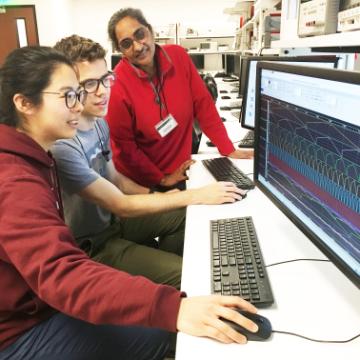
For their capstone project, electrical engineering seniors Bradford Kidd and Anne Hsia have stepped up to address the challenge of stepping down the regulation of power in IoT devices. The pair have designed a device that reduces the physical footprint and the power consumption of traditional voltage converters. They started by reading stacks of academic journals and Ph.D. dissertations to gain insight into how to proceed. “We are doing something new that really isn’t taught in school,” said Brad. “We knew we needed something ridiculously small, less than one square millimeter, so we decided to create an integrated circuit design that uses switches and capacitors rather than inductors—which are inefficient, have a lot of noise, and are very large—to step down power input as needed.” Their design reduces an input of 0.9–1.3V to 0.6V; perfect for IoT applications.
The design process consisted of, in Brad’s words, “drawing a lot of rectangles”—laying out how their converter would be configured, deciding just how many switches and capacitors were needed, and how the chip would be manufactured. They also had to determine if the switch between frequencies should be linear or logarithmic, and they had to account for parasitics. Ummm…excuse me? Anne explained: “Parasitics are the things that eat away at efficiency. Friction is one problem, but we also had to consider loss from switches or capacitors not operating at 100 percent efficiency, 100 percent of the time.” The pair used feedback flow charts to read which frequency to use and made dozens of graphs to judge how well things were working.
Turns out, their design works really well—operating at 90 percent efficiency for up to 30µA load currents. The team’s advisor, Electrical Engineering Chair and Professor Shoba Krishnan, is thrilled with their work. “This is good old-fashioned engineering design,” she said. “Short of sending their design out to be fabricated, they are doing everything just like they would if they were working for a Silicon Valley company, and their design is actually being used by one of our electrical engineering Ph.D. students for his research.”
The words bring a smile to Brad’s face. “I was looking for a senior design project that was aimed toward where I’m going with my career. I’ve been interested in analog IC design and wanted to create a layout that a company could use in their chip,” he said. Though he is enrolled in electrical engineering’s combined five-year BS/MS degree program and will continue at SCU for another year, Brad has already landed a job with Adesto Technologies.
As for Anne, the classically trained pianist who is triple majoring in EE, mathematics, and music, she’s keeping her options open for the time being. “Working with a teammate and being able to bounce ideas off each other while tackling a very technical project has been great. It was just what I wanted. And creating a design that will be beneficial to chip manufacturers is really fulfilling,” she said.